

Ohms
-
Posts
10 -
Joined
-
Last visited
Content Type
Forums
Store
Crowdfunding
Applications
Events
Raffles
Community Map
Posts posted by Ohms
-
-
When i read the PA_EINT_DEB_REG using devmem2 i get the following:
sudo devmem2 0x01c20a18
/dev/mem opened.
Memory mapped at address 0xb6fa5000.
Value at address 0x1C20A18 (0xb6fa5a18): 0x51Does this mean that the te debounce register is set to the correct oscilator 24MHZ but somthing else has written to the DEB_CLK_PRE_SCALE?
-
I have tried the to place input-debounce = <1 0>; In multiple places in the device tree, as i do not understand exactly were to place it.
I just can not get it to work like this what am i doing wrong?
/dts-v1/;
/ {

...
    counters {
                compatible =  "allwinner,sun8i-h3-pinctrl", "gpio-pulse-counter";
                pi_irq_counter@0 {
                        label = "sst_PA19_pulse_counter";
                        pinctrl-names = "default";
                        pinctrl-0 = <&ext_counter_PA19>;
                        /* CON3, pin 12: PH2 - pin 226 (Multi6 function: EINT2) */
                        /* bank: 226 / 32 = 7, pin into the bank 226 % 32 = 2 */
                        gpios = <&pio 0 19 6>;
                        /* interrupt properties may be omitted if used gpios property */
                        interrupt-parent = <&pio>;
                        interrupt-names = "counter-edge-rising";
                        interrupts = <0 19 0>; /* PA19 / EINT19 / rising edge*/
                        input-debounce = <0x1 0x0>;
                };
        };
        pio: pinctrl@01c20800 {
                        reg = <0x1c20800 0x400>;
                        interrupts = <0x0 0xb 0x4 0x0 0x11 0x4>;
                        clocks = <0x2 0x36 0x3 0x5>;
                        clock-names = "apb", "hosc", "losc";
                        gpio-controller;
                        #gpio-cells = <0x3>;
                        interrupt-controller;
                        #interrupt-cells = <0x3>;
                        compatible = "allwinner,sun8i-h3-pinctrl";
                        linux,phandle = <0xd>;
                        phandle = <0xd>;
                        input-debounce = <0x1 0x0>;
....

                       ext_counter_PA19: sst_pins@0 {
                                allwinner,pins = "PA19";
                                allwinner,function = "gpio_in";
                                allwinner,input-debounce = <1 1>;
                                allwinner,drive = <0>;
                                allwinner,pull = <1>;
                        };
        };
.....

};
-
Gentlemen Thank you very much.
Both solutions work in a similar way by getting the base address from /dev/mem.
By writing 1 to the PA_EINT_DEB_REG which sets HSOSC24MHz on for the debounce filter i managed to get PA19 interrupts working.
# Read PA_EINT_CTL_REG
sudo devmem2 0x01c20a10
/dev/mem opened.
Memory mapped at address 0xb6f87000.
Value at address 0x1C20A10 (0xb6f87a10): 0x80000

#which indicates that PA19 is set to external interrupts (OK)

# Enable HSOSC by writing a 1 to PA_EINT_DEB_REG
sudo devmem2 0x01c20a18 w 1
/dev/mem opened.
Memory mapped at address 0xb6f38000.
Value at address 0x1C20A18 (0xb6f38a18): 0x1
Written 0x1; readback 0x1
I can go as high as 130Khz (which is more than sufficient in my case) after that jitter becomes a problem .
138874405,130857 139005379,130974 139136288,130909 -
Thanks for the help i will give it a try and report back
-
Thanks for the link. But when i try to do low level programming of the registers on mainline kernel, using the code presented in my first post, I get a segmentation fault.
Do you know how to obtain the base address of the registers on mainline kernel?
For legacy kernel 3.4 it is IO_ADDRESS(x) ((x) + 0xf0000000).
-
Yes the interrupts are short if the processor is polling, but this is quite normal for hardware trigger circuits. I looked up the datasheets and it seems that there are 2 frequency modes for input debounce but i have no idea how to set them. I have tried input-debounce = <1>; in the device tree but it makes no difference. Further i see no reference to a higher precision clock. It seems that the H3 is not suitable for this kind of design???
-
Here is a follow up on the latest changes:
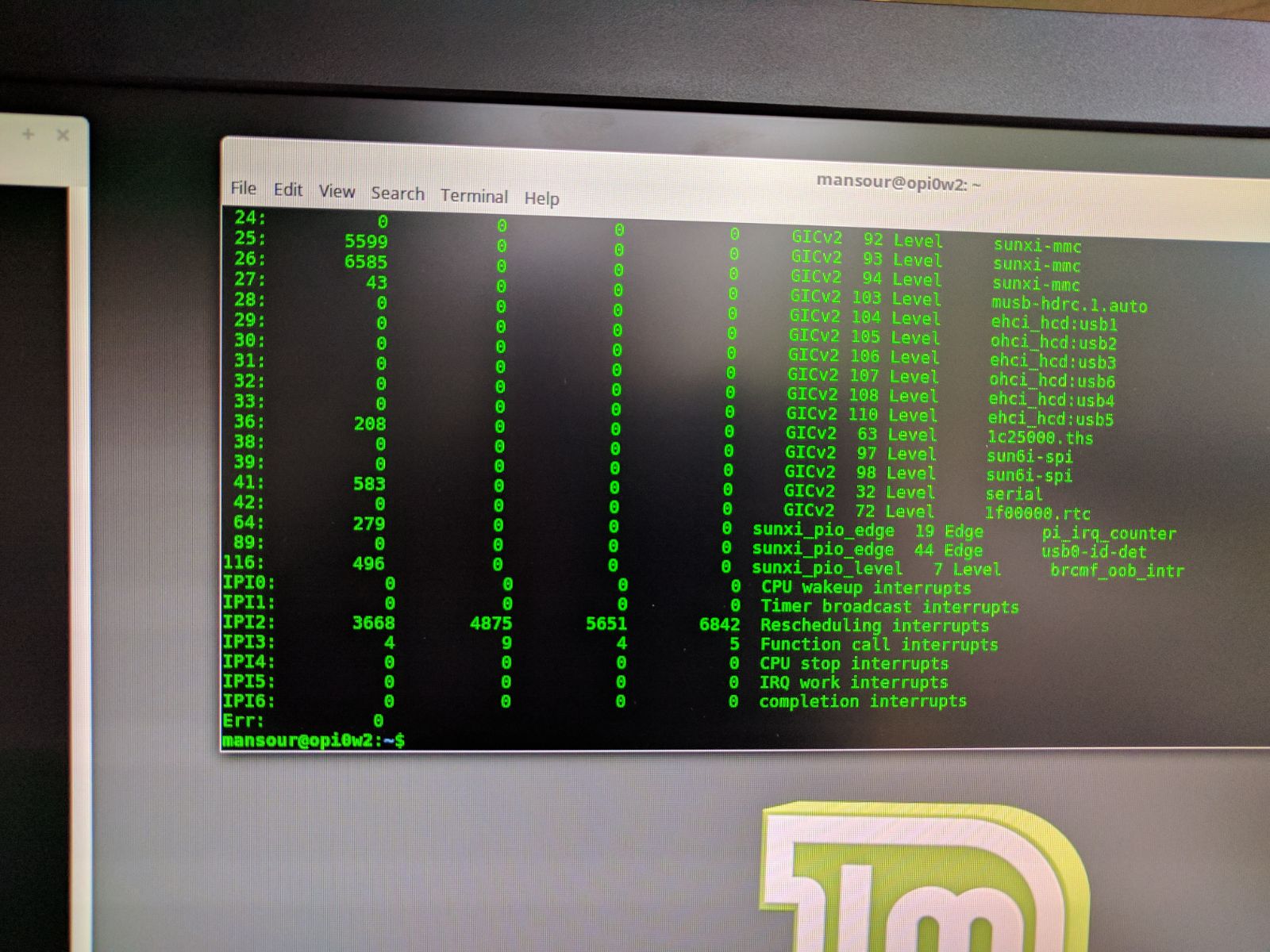
cat /proc/interrupts shows 0 at pi_irq_counter, irq 64
           CPU0       CPU1       CPU2       CPU3
...
 64:          0          0          0          0  sunxi_pio_edge  19 Edge      pi_irq_counter
...
sudo cat /sys/kernel/debug/gpio shows:
gpiochip0: GPIOs 0-223, parent: platform/1c20800.pinctrl, 1c20800.pinctrl:
 gpio-3   (                    |sst:red:led         ) out lo
 gpio-9   (                    |reset               ) out hi
 gpio-17  (                    |orangepi:red:status ) out lo
 gpio-19  (                    |pi_irq_counter      ) in  lo IRQ
 gpio-102 (                    |usb1-vbus           ) out hi
 gpio-107 (                    |sst:blue:led        ) out lo
 gpio-166 (                    |cd                  ) in  hi
 gpio-204 (                    |usb0_id_det         ) in  lo IRQ
Which suggests that gpio-19 was correctly set as an irq pin:
So i went back and tested with function generator by changing frequency and pulse widths and measuring the number of pulses /sec using the following script:
prevCount=0;
while true;
do
  count=`cat /proc/interrupts| grep --color=never 64:|sed "s/^[     ]*64:[  ]*\([0-9]*\)[   ].*$/\1/"`;
  echo $count,$((count-prevCount));
  prevCount=$count;
  sleep 1;
done
here are the results:
dat1.txt: Pulse frequency increase from 50Hz to 8KHz are correct, errors start to occur above 8KHz
dat2.txt: Changed pulse duty cycle from 50% to 1%, frequency 450Hz, errors start to occur below 2% pwm duty cycle
What do i need to change in order to capture the ADC pulses which have a pulse width of 1us?
any help please!!!
-
Ok i will give it a try an report back.
Thanks for the tip.
-
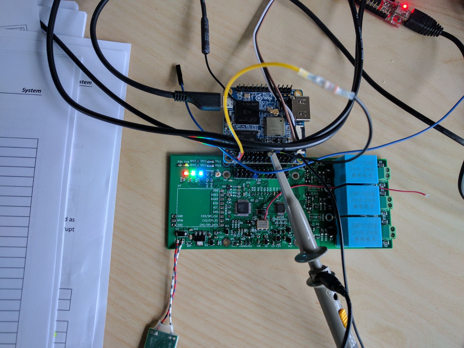
Recently i have been experimenting with interrupts on orange pi zero plus2-H3 trying to capture data-ready pulses from an external adc on gpio PA19. The aim is to synchronize spi-read-data transactions with the incoming adc data-ready signal. First I tried to get it to work on legacy kernel 3.4 by adding the following section in to /boot/script.fex and compile the .fex file to .bin file using fex2bin:
[gpio_para]
gpio_used = 1
gpio_num = 6
....
gpio_pin_6 = port:PA19<0><default><default><1>
This configured the pin properly as i had tested on other pins with some leds and it works. The driver code for capturing the interrupt was based on an example i found at https://github.com/tomxue/Kernel_GPIO_interrupt/blob/master/m_test.c and is as follows:
...

#define GPIO_PIN 19
#define GPIO_PIN_DESC "GPIO PA19 interrupt test"

static irqreturn_t r_irq_handler(int irq, void *dev_id, struct pt_regs *regs) {
   unsigned long flags;

   local_irq_save(flags);
   printk("Interrupt [%d] on device [%s] was triggered!!\n", irq, (char *) dev_id);
   local_irq_restore(flags);

   return IRQ_HANDLED;
}

void config_interrupt (void) {
   int err;
   int gpio_irq;

   err = setup_pinmux();
   if (err < 0) {
      printk("GPIO setup pinmux failure: %s\n", GPIO_PIN_DESC);
      return;
   }

   if (gpio_request(GPIO_PIN, GPIO_PIN_DESC)) {
      printk("GPIO request failure: %s\n", GPIO_PIN_DESC);
      return;
   }

   if (gpio_direction_input(GPIO_PIN)) {
      printk("GPIO set direction input failure %s\n", GPIO_PIN_DESC);
      return;
   }

   if ( (gpio_irq = gpio_to_irq(GPIO_PIN)) < 0 ) {
      printk("GPIO to IRQ mapping failure %s\n", GPIO_PIN_DESC);
      return;
   }

   printk(KERN_NOTICE "Mapped int %d\n", gpio_irq);

   if (request_irq(gpio_irq,
                   (irq_handler_t ) r_irq_handler,
                   IRQF_TRIGGER_RISING,   // IRQF_TRIGGER_LOW,
                   GPIO_PIN_DESC,
                   GPIO_PIN_DEVICE_DESC)) {
      printk("Irq Request failure\n");
      return;
   }

   return;
}
Unfortunately i could only get it to work if i replace IRQF_TRIGGER_RISING with IRQF_TRIGGER_LOW. This was tested by issuing dmesg to obtain the irq number and then cat /proc/interrupts to monitor interrupt events on the allocated irq. At first, this gave me the impression that interrupts in the kernel are polling the pin instead of actual hardware triggering. Based on the data sheets of the sunxi H3 chipset (http://dl.linux-sunxi.org/H3/Allwinner_H3_Datasheet_V1.0.pdf, page 74) PA19 is interrupt capable by the setting the pinmux to PA_EINT19, function code 0x6. So i decided to do low level configuration of the pinmux by adding the following section to the module and test accordingly:
/**
 * Low level configuration of GPIO pin mode
 */
#ifdef KERNEL_34
#define IOMEM(x) ((void __force __iomem *)(x))
#ifndef IO_ADDRESS
#define IO_ADDRESS(x) ((x) + 0xf0000000)
#endif
#ifndef __io_address
#define __io_address(n) IOMEM(IO_ADDRESS(n))
#endif


// IO memory map base address, discovered by searching through Armbian sources
#define SUNXI_IOMEM(n) (0xf0000000 + (n))
#define PIO_BASE SUNXI_IOMEM(0x01C20800)

// gpio banks of the ALLWINNER H3
#define GPIO_BANK_A 0
//#define GPIO_BANK_B 1        // not a valid bank on H3
#define GPIO_BANK_C 2
#define GPIO_BANK_D 3
#define GPIO_BANK_E 4
#define GPIO_BANK_F 5
#define GPIO_BANK_G 6

// PORT configuration registers
#define Pn_CFG0_REG(n)        (PIO_BASE + (n*0x24) + (0x00))    // 32bits[0..31] see data sheet
#define Pn_CFG1_REG(n)        (PIO_BASE + (n*0x24) + (0x04))
#define Pn_CFG2_REG(n)        (PIO_BASE + (n*0x24) + (0x08))
#define Pn_CFG3_REG(n)        (PIO_BASE + (n*0x24) + (0x0c))

#define PA_DAT                (PIO_BASE + 0x10)
#define PA_PULL               (PIO_BASE + 0x1C)

#define PA_EINT_CFG_REG(n)    (PIO_BASE + 0x200 + (4*n))
#define PA_EINT_CTL_REG       (PIO_BASE + 0x210)
#define PA_EINT_STATUS_REG    (PIO_BASE + 0x214)
#define PA_EINT_DEB_REG       (PIO_BASE + 0x218)

#define readb(addr)        (*((volatile unsigned char  *)(addr)))
#define readw(addr)        (*((volatile unsigned short *)(addr)))
#define readl(addr)        (*((volatile unsigned long  *)(addr)))
#define writeb(v, addr)    (*((volatile unsigned char  *)(addr)) = (unsigned char)(v))
#define writew(v, addr)    (*((volatile unsigned short *)(addr)) = (unsigned short)(v))
#define writel(v, addr)    (*((volatile unsigned long  *)(addr)) = (unsigned long)(v))
#endif


#ifdef KERNEL_34
static int setup_pinmux(void) {
    int cfg;
    int shift;
    unsigned int val = 0x6 ;    // function 0x6  = PA_EINT mode
    unsigned int reg, mask;

    //writel(0x00711112, Pn_CFG2_REG(GPIO_BANK_A));  // default register value

    void __iomem *base = __io_address(0x01c28000);
    printk("GPIO: base                     = 0x%lx, %s \n", (long unsigned int)base, GPIO_PIN_DESC);
    printk("GPIO: PIO_BASE                 = 0x%lx, %s \n", (long unsigned int)PIO_BASE, GPIO_PIN_DESC);

    // display CFG registers of GPIO_BANK_A
    printk("GPIO: Pn_CFG0_REG(GPIO_BANK_A) = 0x%.8lx, %s \n", readl(Pn_CFG0_REG(GPIO_BANK_A)), GPIO_PIN_DESC);
    printk("GPIO: Pn_CFG1_REG(GPIO_BANK_A) = 0x%.8lx, %s \n", readl(Pn_CFG1_REG(GPIO_BANK_A)), GPIO_PIN_DESC);
    printk("GPIO: Pn_CFG2_REG(GPIO_BANK_A) = 0x%.8lx, %s \n", readl(Pn_CFG2_REG(GPIO_BANK_A)), GPIO_PIN_DESC);
    printk("GPIO: Pn_CFG3_REG(GPIO_BANK_A) = 0x%.8lx, %s \n", readl(Pn_CFG3_REG(GPIO_BANK_A)), GPIO_PIN_DESC);
    //
    printk("GPIO: PA_DAT             = 0x%.8lx, %s \n", readl(PA_DAT),            GPIO_PIN_DESC);
    printk("GPIO: PA_PULL            = 0x%.8lx, %s \n", readl(PA_PULL),            GPIO_PIN_DESC);
    printk("GPIO: PA_EINT_STATUS     = 0x%.8lx, %s \n", readl(PA_EINT_STATUS_REG), GPIO_PIN_DESC);
    printk("GPIO: PA_EINT_DEB_REG    = 0x%.8lx, %s \n", readl(PA_EINT_DEB_REG),    GPIO_PIN_DESC);
    printk("GPIO: PA_EINT_CFG_REG(0) = 0x%.8lx, %s \n", readl(PA_EINT_CFG_REG(0)),GPIO_PIN_DESC);
    printk("GPIO: PA_EINT_CTL_REG    = 0x%.8lx, %s \n", readl(PA_EINT_CTL_REG),    GPIO_PIN_DESC);

    printk("GPIO: writing to registers, %s \n", GPIO_PIN_DESC);

    //set PA19_SELECT to PA_EIN19
    // PAn_SELECT(GPIO_BANK_A, 19, 0x6);
    // bank  = (19*4)/32 = 2 = PA_CFG2
    // shift = (19*4)-(bank*32)/4
    cfg = (GPIO_PIN * 4) / 32;
    shift = ((GPIO_PIN * 4) - (cfg * 32)) ;
    mask = ~(0x0000000f << shift);
    val = val << shift;
    printk("GPIO: cfg=%d, shift=%d, mask=0x%.8lx,  %s \n", cfg, shift, mask, GPIO_PIN_DESC);
    switch (cfg){
    case 0:
        reg = readl(Pn_CFG0_REG(GPIO_BANK_A));
        reg &= mask;
        reg |= val;
        writel(reg, Pn_CFG0_REG(GPIO_BANK_A));
        break;
    case 1:
        reg = readl(Pn_CFG1_REG(GPIO_BANK_A));
        reg &= mask;
        reg |= val;
        writel(reg, Pn_CFG1_REG(GPIO_BANK_A));
        break;
    case 2:
        reg = readl(Pn_CFG2_REG(GPIO_BANK_A));
        reg &= mask;
        reg |= val;
        writel(reg, Pn_CFG2_REG(GPIO_BANK_A));
        break;
    case 3:
        reg = readl(Pn_CFG3_REG(GPIO_BANK_A));
        reg &= mask;
        reg |= val;
        writel(reg, Pn_CFG3_REG(GPIO_BANK_A));
        break;
    }
    printk("GPIO: Pn_CFG0_REG(GPIO_BANK_A) = 0x%.8lx, %s \n", readl(Pn_CFG0_REG(GPIO_BANK_A)), GPIO_PIN_DESC);
    printk("GPIO: Pn_CFG1_REG(GPIO_BANK_A) = 0x%.8lx, %s \n", readl(Pn_CFG1_REG(GPIO_BANK_A)), GPIO_PIN_DESC);
    printk("GPIO: Pn_CFG2_REG(GPIO_BANK_A) = 0x%.8lx, %s \n", readl(Pn_CFG2_REG(GPIO_BANK_A)), GPIO_PIN_DESC);
    printk("GPIO: Pn_CFG3_REG(GPIO_BANK_A) = 0x%.8lx, %s \n", readl(Pn_CFG3_REG(GPIO_BANK_A)), GPIO_PIN_DESC);

the    // enable interrupt on PA19
    reg = readl(PA_EINT_CTL_REG);
    reg |= 1 << GPIO_PIN;
    writel(reg, PA_EINT_CTL_REG);
    printk("GPIO: PA_EINT_CTL_REG    = 0x%.8lx, %s \n", readl(PA_EINT_CTL_REG),    GPIO_PIN_DESC);
    printk("GPIO: PA_EINT_STATUS     = 0x%.8lx, %s \n", readl(PA_EINT_STATUS_REG), GPIO_PIN_DESC);

   return 0;
}
#endif
I could see in the dmesg printouts that the PA19-pin was configured properly but still i could only get interrupts to work if i use IRQF_TRIGGER_LOW.After some reading on the Internet and instability issues with WiFi i decided to go with the latest mainline development kernel which uses device trees. Executing the kernel module with low-level register programming on the mainline kernel resulted in Kernel-oops and segmentation faults.
I modified /boot/dtb/sun8i-h3-orangepi-zeroplus.dts based on an example i found at http://geek-mag.com/posts/265668/ as follows and tested using the pulse-counter module presented at the same site:
/dts-v1/;
/ {
    interrupt-parent = <0x1>;
    #address-cells = <0x1>;
    #size-cells = <0x1>;
    model = "Xunlong Orange Pi Zero Plus";
    compatible = "xunlong,orangepi-zeroplus", "allwinner,sun8i-h3";

    sst: pulse_counter {
       compatible = "gpio-pulse-counter";
       pi_irq_counter@0 {
          label = "sst_PA19_pulse_counter";
          pinctrl-names = "default";
          pinctrl-0 = <&ext_counter_PA19>;

          /* bank: 0, pin 19, function 6 */
          gpios = <&pio 0 19 6>;

          /* interrupt properties may be omitted if used gpios property */
          interrupt-parent = <&pio>;
          interrupt-names = "counter-edge-rising";
          interrupts = <19 0>; /* PA19 / EINT19 / rising edge*/
      };
   };

....

   pio: pinctrl@01c20800 {
         reg = <0x1c20800 0x400>;
         interrupts = <0x0 0xb 0x4 0x0 0x11 0x4>;
         clocks = <0x2 0x36 0x3 0x5>;
         clock-names = "apb", "hosc", "losc";
         gpio-controller;
         #gpio-cells = <0x3>;
         interrupt-controller;
         #interrupt-cells = <0x3>;
         compatible = "allwinner,sun8i-h3-pinctrl";
         linux,phandle = <0xd>;
         phandle = <0xd>;

....

         ext_counter_PA19: sst_pins@0 {
              allwinner,pins = "PA19";
              allwinner,function = "gpio_in";
              drive = <0>;
              pull = <1>;
        };
   };
};
Still the same issues, I could only get interrupts if i set IRQF_TRIGGER_LOW. After three weeks of reading, digging and diving on the Internet i had decided to test gpio-PA19 using a switch connected with a pull-up resistor to 3.3v. pressing the switch will result in grounding PA19 and hence a rising edge pulse will be generated when the switch is released. To my surprise i got rising edge interrupts to work. Now y thaughts are shifting towards hardware issues so i grabbed a scope and function generator to monitor the activities on the gpio-pin PA19.
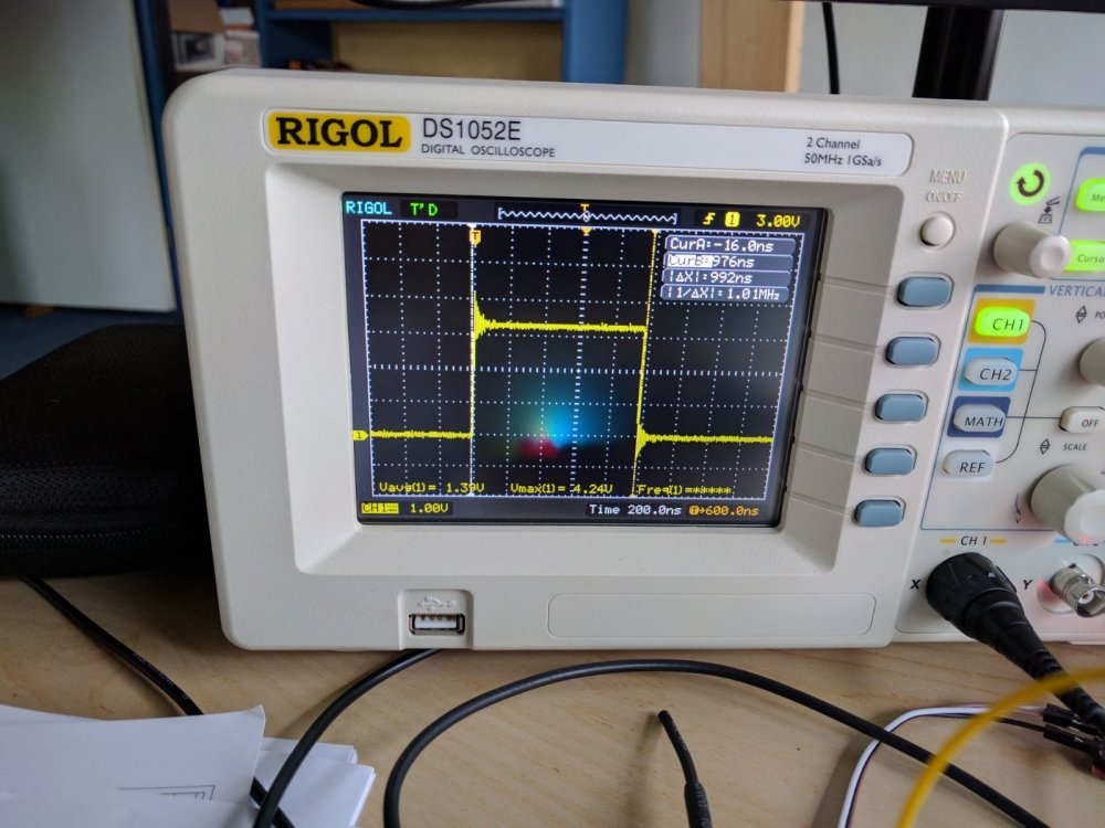
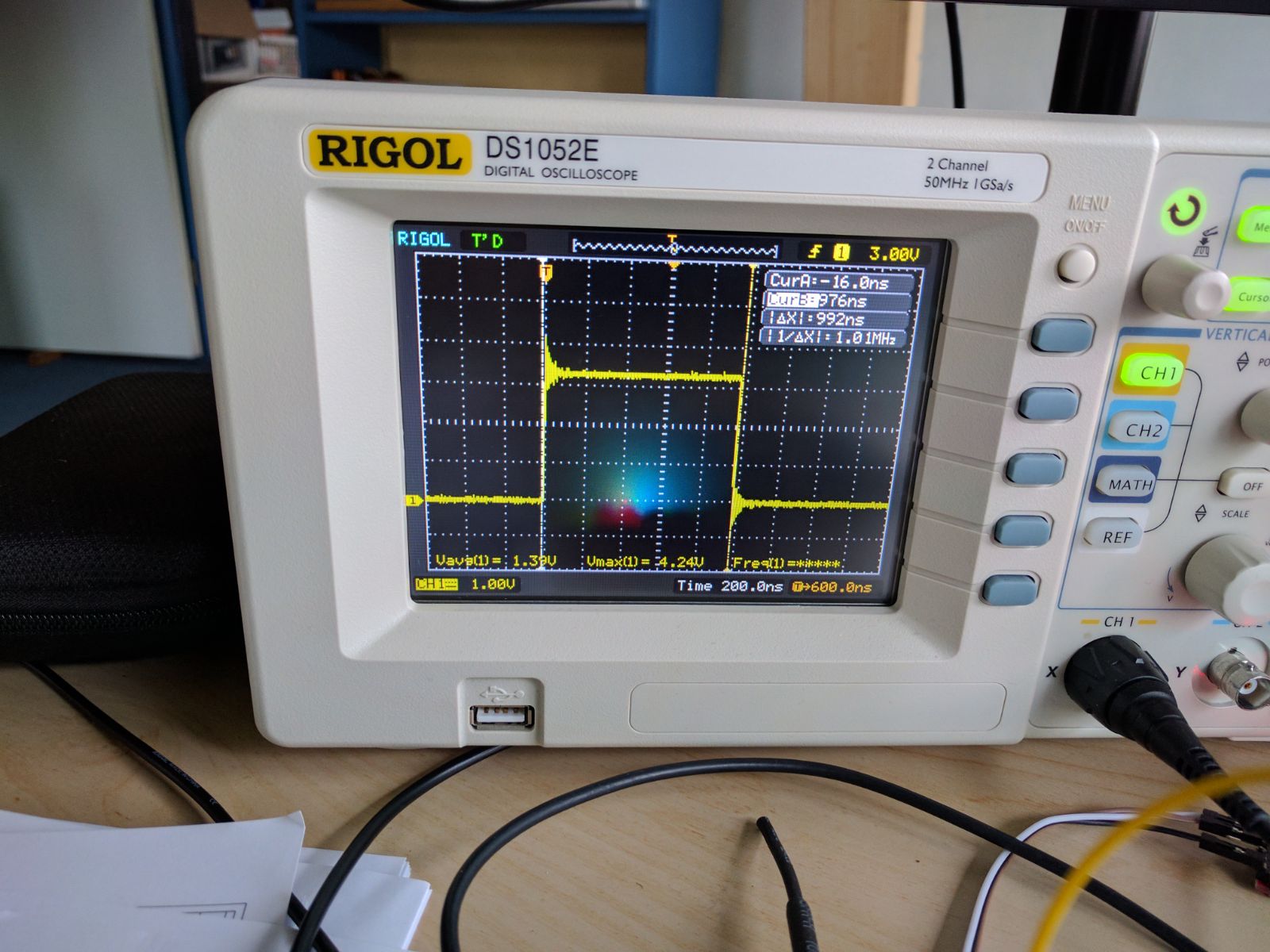
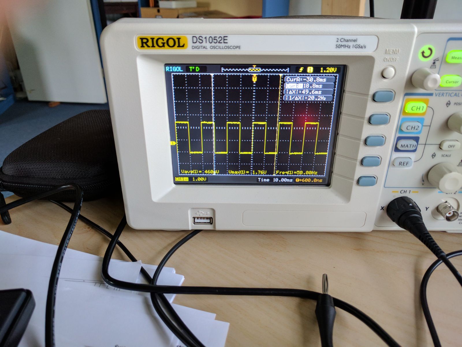
Here are some of my findings:- Picture 1: adc_drdy_pulse_width.jpeg, pulse width 1us, frequency 2KHz - 128Khz depending on sampling frequency setup, no-interrupts detected
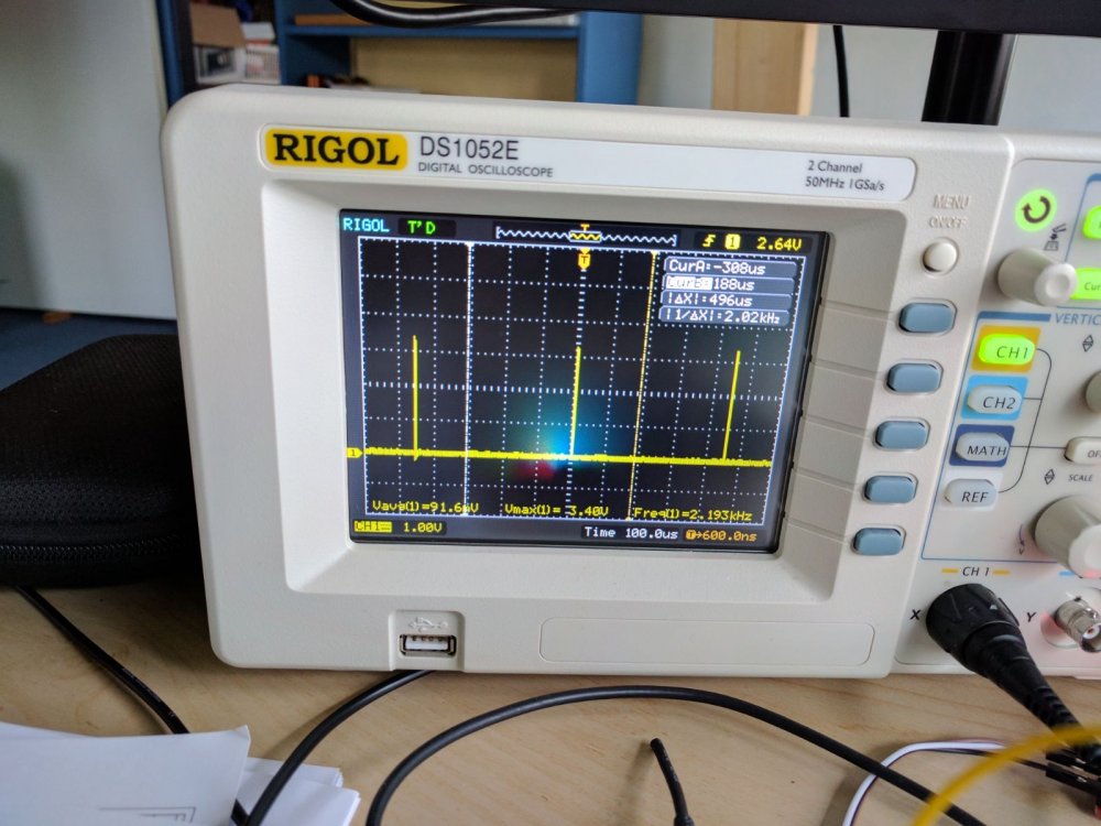
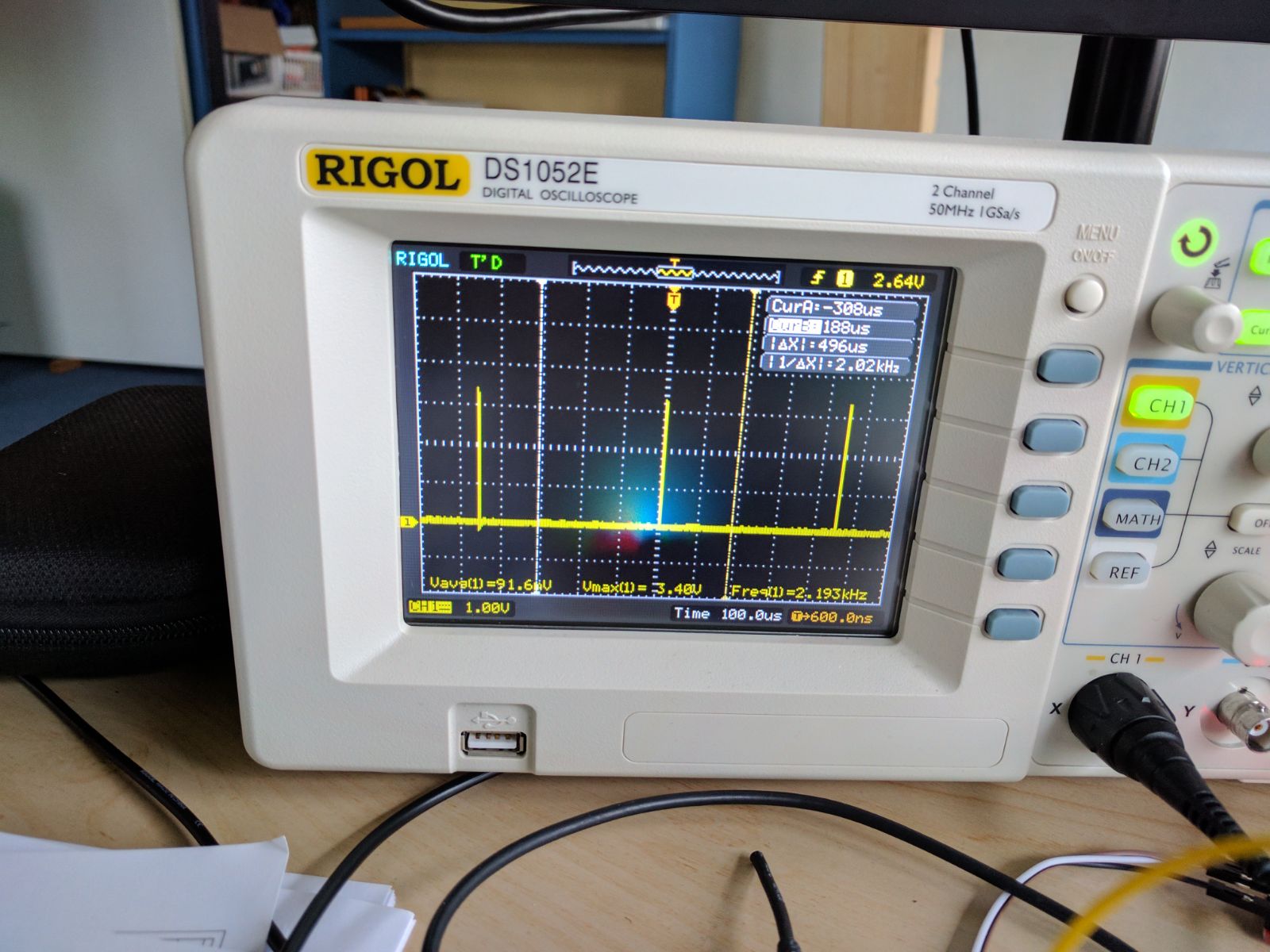
- Picture 2: adc-pulse-frequency.jpeg
- Picture 3: function-generator-pulse-50percent-duty.jpeg, frequency 50Hz, interrupts visible if i increase generator voltage to 4.3 volts. It seems that the gpio input load reduces the function-generator voltage from 3.3V to 2.7V and hence logic level voltages are not detected correctly.
Conclusions:
interrupt activity detection is lowered as the frequency increases
@10KHz no more interrupts visible
@1% pulse duty cycle of 400Hz no more interrupts visible
Questions:
1) How do i activate hardware irq sampling on PA19 in mainline kernel?
2) How do i set irq-pin sampling debounce to 24MHz on mainline kernel?
3) Can the kernel handle high speed irq's4) Why does are irqs not triggering when i increase the pulse frequency or lower pwm duty.
5) How can i do low level register programming in mainline kernel?
Any help would be appreciated


DMA configuration for SPI not used in mainline
in Allwinner sunxi
Posted
From your description it seems that the function dma_set_mask_and_coherent() which used to work for kernel version 4.13.3 and no longer for newer kernel versions?
That's a shame, Have you checked the release notes of newer kernel versions with sunxi modifications or maybe some of the experts on this forum can react?